JTAGulator: Assisted discovery of on-chip debug interfaces

JTAGulator
On-chip debug (OCD) interfaces can provide chip-level control of a target device and are a primary vector used by engineers, researchers, and hackers to extract program code or data, modify memory contents or affect device operation on-the-fly. Depending on the complexity of the target device, manually locating available OCD connections can be a difficult and time-consuming task, sometimes requiring physical destruction or modification of the device.
Designed by Grand Idea Studio, the JTAGulator is an open-source hardware tool that assists in identifying OCD connections from test points, vias, or component pads on a target device.
Features
- Detection of JTAG/IEEE 1149.1, ARM SWD, and UART/asynchronous serial
- Direct connection to sigrok and OpenOCD
- 24 channels with input protection circuitry
- Adjustable target I/O voltage for level translation: 1.4V to 3.3V
- USB interface (FTDI FT232) for menu-based control from a host computer (Windows, macOS, Linux)
The JTAGulator is powered from the host computer’s USB port and uses an industry-standard FTDI FT232RL device to provide the USB connectivity. The device will appear as a Virtual COM port and will have a COM port or device tty automatically assigned to it.
All communication is 115200 bps, 8 data bits, no parity, 1 stop bit. Use a terminal program (for example, PuTTY, CoolTerm, minicom/picocom, or screen) to communicate with the JTAGulator.
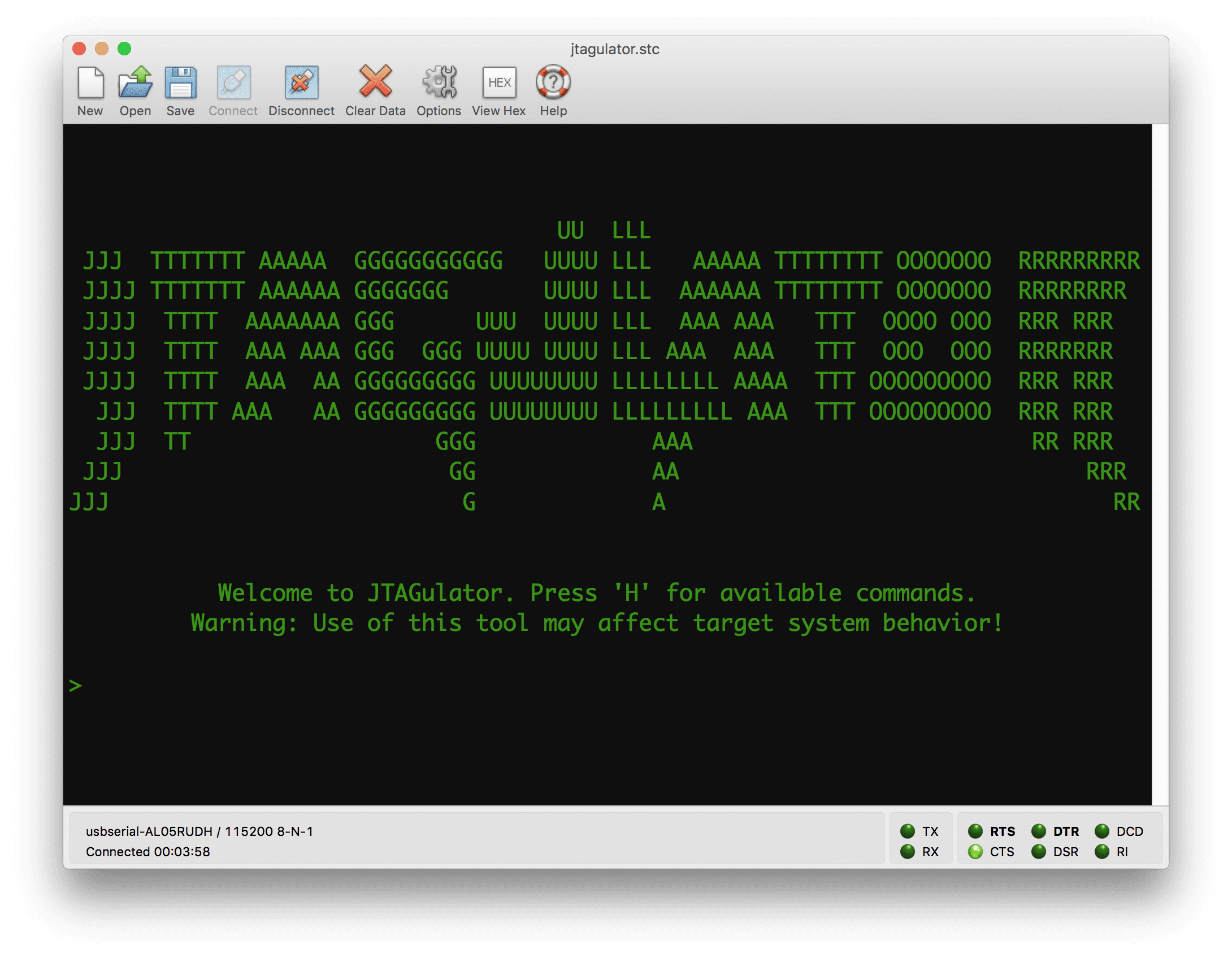
Upon successful connection to a host, the JTAGulator’s LED will turn YELLOW and it will wait until the user presses any key from within the terminal program. The JTAGulator will then send its welcome header and command prompt.
When the JTAGulator is ready to receive commands, it will send a > to the host and the LED will turn GREEN. It will then wait in an idle state until it receives a valid command, at which time it performs the command and returns any command-specific response. If an invalid command is received, the JTAGulator will respond with a ?.
Set the target I/O voltage (VADJ) using the V command. This will ensure that the target receives signals within its acceptable logic levels. The voltage can be determined by locating and measuring VCC on the target board or by checking the datasheet of the specific component to which you will be connecting (if known).
Attach the target’s points to the JTAGulator using the screw-in terminal blocks or via the 2×5 male headers, starting at CH0 and incrementing sequentially as needed. Ensure there is a shared GND connection between the JTAGulator and the target board. VADJ should not be connected to the target board (it is made available on the headers for testing and future use). The 2×5 headers are compatible with Bus Pirate probes and 0.1″ jumper wires.
The JTAGulator’s input protection circuitry allows a maximum input voltage of VADJ +/- 12.5V for each channel pin. Exceeding this value may cause damage to on-board components.


